132BGA
https://www.krystaic.com/product/embedded-chips/bga132.html
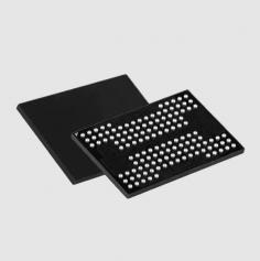
BGA package flash memory, where BGA is the abbreviation of "Ball Grid Array", that is, ball grid array packaging technology, which is the use of ball grid array contact communication. The contact is located at the bottom of the chip. The number of common contacts are 132 or 152. The SMT is soldered by the controlled collapse chip method, which improves its electrical and thermal properties, and the assembly can be co-planar soldered, making it much more reliable.
For future PCIE 4.0 SSDs, higher transfer rates can only be achieved with BGA packages. In the future, all flash memory in BGA packages will be used in both the consumer and enterprise sectors, instead of TSOP package.
